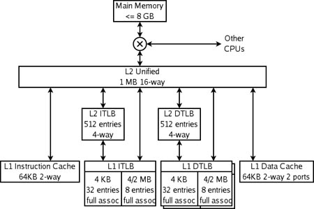
here is the cache hierarchy of the AMD Athlon64
The K8 has 4 specialized caches: an instruction cache, an instruction TLB, a data TLB, and a data cache. Each of these caches is specialized:
The instruction cache keeps copies of 64 byte lines of memory, and fetches 16 bytes each cycle. Each byte in this cache is stored in ten bits rather than 8, with the extra bits marking the boundaries of instructions (this is an example of predecoding). The cache has only parity protection rather than ECC, because parity is smaller and any damaged data can be replaced by fresh data fetched from memory (which always has an up-to-date copy of instructions).
The instruction TLB keeps copies of page table entries (PTEs). Each cycle's instruction fetch has its virtual address translated through this TLB into a physical address. Each entry is either 4 or 8 bytes in memory. Each of the TLBs is split into two sections, one to keep PTEs that map 4KB, and one to keep PTEs that map 4MB or 2MB. The split allows the fully associative match circuitry in each section to be simpler. The operating system maps different sections of the virtual address space with different size PTEs.
The data TLB has two copies which keep identical entries. The two copies allow two data accesses per cycle to translate virtual addresses to physical addresses. Like the instruction TLB, this TLB is split into two kinds of entries.
The data cache keeps copies of 64 byte lines of memory. It is split into 8 banks (each storing 8KB of data), and can fetch two 8-byte data each cycle so long as those data are in different banks. There are two copies of the tags, because each 64 byte line is spread among all 8 banks. Each tag copy handles one of the two accesses per cycle.
The K8 also has multiple-level caches. There are second-level instruction and data TLBs, which store only PTEs mapping 4KB. Both instruction and data caches, and the various TLBs, can fill from the large unified L2 cache. This cache is exclusive to both the L1 instruction and data caches, which means that any 8-byte line can only be in one of the L1 instruction cache, the L1 data cache, or the L2 cache. It is, however, possible for a line in the data cache to have a PTE which is also in one of the TLBs—the operating system is responsible for keeping the TLBs coherent by flushing portions of them when the page tables in memory are updated.
The K8 also caches information that is never stored in memory—prediction information. These caches are not shown in the above diagram. As is usual for this class of CPU, the K8 has fairly complex branch prediction, with tables that help predict whether branches are taken and other tables which predict the targets of branches and jumps. Some of this information is associated with instructions, in both the level 1 instruction cache and the unified secondary cache.
The K8 uses an interesting trick to store prediction information with instructions in the secondary cache. Lines in the secondary cache are protected from accidental data corruption (e.g. by an alpha particle strike) by either ECC or parity, depending on whether those lines were evicted from the data or instruction primary caches. Since the parity code takes fewer bits than the ECC code, lines from the instruction cache have a few spare bits. These bits are used to cache branch prediction information associated with those instructions. The net result is that the branch predictor has a larger effective history table, and so has better accuracy.
对于K8来说,AMD历来重视L1,64K Ins+64K Dat,2路组相联的设计让AMD拥有高命中率和低延迟的L1。然而在Instrution Cache中AMD的设计思路又与其它CPU有所不同。首先其Ins中并不存储传统的X86指令,而是存储着分支预测出来的X86指令的信息。再根据这些信息将指令解码成1~2条“宏操作”来执行。由于AMD CPU采用了3条流水线的超标量结构,因此其可以保证同时执行6条这样的宏操作。显然,相比之下AMD CPU的指令执行效率要优于Intel,因此就可以解释为什么AMD 2.4G可以打败Intel 3.2G了。 然而从这样的L1设计来看,似乎和Intel有些异曲同工之妙。
对于L2,AMD历来只有很少的256K或512K。这是由于AMD的Cache设计思想所致。在一般的Cache中,下级Cache总是要保留一个上级Cache的映象,即L1中的数据在L2中也能够找到。L2在L3中亦能够找到相同数据。然而AMD并没有这样做,它的L2中保存的数据都是L1中替换下来的,以保证CPU在下次使用中能够在L2中找到。因此,AMD的Cache结构呈现出L1+L2(L1与L2没有交集)的“怪异”现像,它的L2对于整体性能并不起决定性作用。Sempron 2600+(128K L2)同2800+(256K L2)性能相同,就是这个原因。
目前而言,英特尔拥有相对庞大得多的产能,因此在产品上喜欢加入较大容量的L2 cache,而AMD则希望以较小的L2 cache配合内建的内存控制器来获取适宜的性能/价格平衡,这也是当初加入AMD的DEC处理器研发人员所喜欢的架构策略。
L2 cache再大也是难以避免命中失败,当初DEC的Alpha处理器研发人员就一直很渴望把这样的损失透过集成内存控制器降低到最低。从性能角度出发,无疑是值得鼓励的。
AMD L2不重要之Q&A:
Q:为什么K8 CPU的二级缓存不大却性能强劲?甚至只有Prescott架构(1MB或者2MB 2LCahce)的一半。
A:前言:在酷睿2推出之前,长达一年半的时间AMD占据了CPU性能的绝对优势。
抛开流水线长度比较短、分支预测方式以及集成内存控制器不说。K8架构采用了与Intel Pentium不同的Cache设计思想。在一般Cache中,下级Cache总是要保留一个上一级Cache的缓存,即L1中的数据在L2中能够找到,同样L2中的数据在L1中也可以找到(服务器CPU以及第四季度即将发布的K8L中将集成L3,很早以前,Intel在其工作站版PC解决方案中也包含L3,但那是集成于主板之上的。)然而AMD却没有这样做,它的二级缓存中保留的数据都是L1中替换下来的,这样CPU在下次使用中通过优先访问L2大大提高了效率--因为用户以及OS的操作往往是几个固定进程之间的彼此切换以及对内存中程序数据段的调用集中于小块区域。当然前述部分功能Intel也实现了。但是AMD的Cache结构是以怪异的“L1+L2”(L1/2没有交集)呈现在我们面前的,它的L2对于整体性能并不起决定性作用。所以,桌面版闪龙2800+的L2比闪龙2600+的小(前者256K后者128K)但是2800+的性能却更加强劲(不仅仅是因为频率提高了200MHz,还因为二级缓存对于AMD来说并不重要);所以,移动版的闪龙比Celeron-M更加强劲,Celeron-M因为二级缓存由Pentium-M的1M、2M降到512KB性能大大降低。
没有评论:
发表评论