author:nforcex
AMD(TM)HVM should work with all CPU's in the AMD-V (SVM) series. The desktop processors must be for the "socket AM2" with DDR2 and F2 stepping that are not Sempron brand.
看这则英文资料,所有AM2接口的采用F2步进同时不是闪龙的CPU全部支持代号为Pacifica的AMD-V硬件虚拟化功能。
The list:
* Athlon™ 64 3800+
* Athlon™ 64 3500+
* Athlon™ 64 3200+
* Athlon™ 64 3000+
* Athlon™ 64 FX-62
* Athlon™ 64 FX-70(Quad FX Platform)
* Athlon™ 64 FX-72(Quad FX Platform)
* Athlon™ 64 FX-74(Quad FX Platform)
* Athlon™ 64 X2 Dual-Core 5000+
* Athlon™ 64 X2 Dual-Core 4800+
* Athlon™ 64 X2 Dual-Core 4600+
* Athlon™ 64 X2 Dual-Core 4400+
* Athlon™ 64 X2 Dual-Core 4200+
* Athlon™ 64 X2 Dual-Core 4000+
* Athlon™ 64 X2 Dual-Core 3800+
* Turion(TM) 64 X2 TL-60
* Turion(TM) 64 X2 TL-56
* Turion(TM) 64 X2 TL-52
* Turion(TM) 64 X2 TL-50
the Opteron which is:
* 1000 Series
* 2000 Series
* 8000 Series
而支持VT也就是Intel相应硬件虚拟机功能的CPU列表如下:
* Intel® 2 Core(TM) Duo Extreme processor X6800
* Intel® 2 Core(TM) Duo processor E6700
* Intel® 2 Core(TM) Duo processor E6600
* Intel® 2 Core(TM) Duo processor E6400
* Intel® 2 Core(TM) Duo processor E6300
* Intel® Core(TM) Duo processor T2600
* Intel® Core(TM) Duo processor T2500
* Intel® Core(TM) Duo processor T2400
* Intel® Core(TM) Duo processor L2300
* Intel® Pentium® processor Extreme Edition 965
* Intel® Pentium® processor Extreme Edition 955
* Intel® Pentium® D processor 960
* Intel® Pentium® D processor 950
* Intel® Pentium® D processor 940
* Intel® Pentium® D processor 930
* Intel® Pentium® D processor 920
* Intel® Pentium® 4 processor 672
* Intel® Pentium® 4 processor 662
* Intel® Xeon® processor 7041
* Intel® Xeon® processor 7040
* Intel® Xeon® processor 7030
* Intel® Xeon® processor 7020
* Intel® Xeon® processor 5080
* Intel® Xeon® processor 5063
* Intel® Xeon® processor 5060
* Intel® Xeon® processor 5050
* Intel® Xeon® processor 5030
Intel® Virtualization Technology requires a computer system with an enabled Intel® processor, BIOS, virtual machine monitor (VMM) and for some uses, certain platform software enabled for it. Functionality,performance or other benefits will vary depending on hardware andsoftware configurations. Intel Virtualization Technology-enabled BIOS and VMM applications are currently in development.
看上文,Intel公司资料里说的是些废话,就是说该技术的运作需要相应CPU、BIOS、和虚拟机软件来支持。
2007年5月14日星期一

有这样的同学,幸甚、幸甚
author:nforcex
昨天某同学到我家一起做游戏设计。做完聊天,彼此天南地北的胡侃,知道了很多有趣和生动的事情。她是一名大学辅导员,在处理班务的时候,她总是站在真正是非曲直的角度,站在学生的角度。看起来很像《极道鲜师Ⅱ》上的 山口久美子,并且一样是年轻的女老师[跟学生几乎一样大],同时也是 a bit beautiful。
领导向她施压要她评优评奖学金照顾走关系的人,她置之不理;学生只要不是真的人品不好或做错了什么可以跟她开玩笑,还能跟着她蹭饭;偶然自己的手机打错电话对方知道她是女的疯狂骚扰,她找一帮学生反过来恶搞那个男的,还骗他到世纪欢乐园放了一下午鸽子;同事生病了会跑去照顾;最看不起那些不靠自己本事只会混关系耍深沉打酒令的人~~~~~~~
也许在中国,这个人脉关系当道的社会,作为成人不得不妥协。但是我仍然敬仰敬佩我的这位真性情的同学。
有这样的同学,并且可以做朋友,真是幸甚、幸甚。
昨天某同学到我家一起做游戏设计。做完聊天,彼此天南地北的胡侃,知道了很多有趣和生动的事情。她是一名大学辅导员,在处理班务的时候,她总是站在真正是非曲直的角度,站在学生的角度。看起来很像《极道鲜师Ⅱ》上的 山口久美子,并且一样是年轻的女老师[跟学生几乎一样大],同时也是 a bit beautiful。
领导向她施压要她评优评奖学金照顾走关系的人,她置之不理;学生只要不是真的人品不好或做错了什么可以跟她开玩笑,还能跟着她蹭饭;偶然自己的手机打错电话对方知道她是女的疯狂骚扰,她找一帮学生反过来恶搞那个男的,还骗他到世纪欢乐园放了一下午鸽子;同事生病了会跑去照顾;最看不起那些不靠自己本事只会混关系耍深沉打酒令的人~~~~~~~
也许在中国,这个人脉关系当道的社会,作为成人不得不妥协。但是我仍然敬仰敬佩我的这位真性情的同学。
有这样的同学,并且可以做朋友,真是幸甚、幸甚。
2007年5月8日星期二
3D引擎_摘抄
3D (Game) Engine运行在底层平台软件(WIN32 API,OPEN GL ,Direct Sound ,D3D...)上,属于上层的平台软件。对更上层的用户(游戏内容制作者而非程序员)提供一个接口,此类接口使得游戏内容制作者可以通过数据方式(比方表格)而非编程方式,或仅简单的脚本编程,制作游戏。
在3D方面,要将物体数据有组织地存储起来,通常使用DAG(有向无环图)数据结构。要将物体高效的显示出来,就有决定那些是无须画的(不画当然最快),就有BSP法、Portal、普通的CLIP方法等等大量的Culling算法。而物体之间的物理位置信息则要用碰撞检测去处理。
处理表格或脚本要Game Logic单元。预处理游戏者输入要事件响应单元...
可见3D Engine在D3D等上提供了大量的东西。目前的3D Engine仍留有很大的改进余地。全局光照仍无法实时实现。目前的碰撞检测的精度仍太粗糙。阴影的绘制尽管由于硬件的发展而产生了长足的进步,但仍无法做到速度与质量双满意...
总之,画三角形不难;把软件面对芯片架构优化以画的快一些也不是大题目。难得是能管理复杂场景,并将其高效、漂亮地画出来。这就是3D Engine要干的。
在3D方面,要将物体数据有组织地存储起来,通常使用DAG(有向无环图)数据结构。要将物体高效的显示出来,就有决定那些是无须画的(不画当然最快),就有BSP法、Portal、普通的CLIP方法等等大量的Culling算法。而物体之间的物理位置信息则要用碰撞检测去处理。
处理表格或脚本要Game Logic单元。预处理游戏者输入要事件响应单元...
可见3D Engine在D3D等上提供了大量的东西。目前的3D Engine仍留有很大的改进余地。全局光照仍无法实时实现。目前的碰撞检测的精度仍太粗糙。阴影的绘制尽管由于硬件的发展而产生了长足的进步,但仍无法做到速度与质量双满意...
总之,画三角形不难;把软件面对芯片架构优化以画的快一些也不是大题目。难得是能管理复杂场景,并将其高效、漂亮地画出来。这就是3D Engine要干的。
2007年5月7日星期一
因HD涉及到的系统性能与防震
author:nforcex
1. 无论Desktop PC还是Server,以现有的技术来看,性能瓶颈之所在位于I/O和硬盘。I/O是一个模糊而宽泛的概念,它的性能随着各种接口技术、传输技术的改进在不断提高中。而对于硬盘来说,由于其“机械手臂”这一先天不良的缓慢性导致一直鲜有提高,近7年来硬盘的寻道速度一直保持在8.5ms到10ms之间,没有显著进步。
最近一来,磁盘和主存的速度相差5个数量级,可想而知尽可能少的调用外存是提高速度的重要手段--内存增容、OS预加载常用进程的模块、pagefile.sys移至高速NAND 等等等等。
1. 无论Desktop PC还是Server,以现有的技术来看,性能瓶颈之所在位于I/O和硬盘。I/O是一个模糊而宽泛的概念,它的性能随着各种接口技术、传输技术的改进在不断提高中。而对于硬盘来说,由于其“机械手臂”这一先天不良的缓慢性导致一直鲜有提高,近7年来硬盘的寻道速度一直保持在8.5ms到10ms之间,没有显著进步。
最近一来,磁盘和主存的速度相差5个数量级,可想而知尽可能少的调用外存是提高速度的重要手段--内存增容、OS预加载常用进程的模块、pagefile.sys移至高速NAND 等等等等。
2. 另外,磁盘磁头距离盘片的距离是那样的近以至于它与灰尘高度的比例还要小于1米与从波士顿到加州的距离的比例。所以、、、、、、正在工作业已出鞘的磁头经不起震动,但是停机断电的磁头就好多了(磁头已经收了回去)。所以硬盘被誉为PC系统中最怕震的配件,剩下的也就Monitor了吧。
L1&L2 Cache of the K8(谈为什么AMD CPU的二级缓存不重要?)
author:nforcex
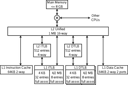
here is the cache hierarchy of the AMD Athlon64
The K8 has 4 specialized caches: an instruction cache, an instruction TLB, a data TLB, and a data cache. Each of these caches is specialized:
The instruction cache keeps copies of 64 byte lines of memory, and fetches 16 bytes each cycle. Each byte in this cache is stored in ten bits rather than 8, with the extra bits marking the boundaries of instructions (this is an example of predecoding). The cache has only parity protection rather than ECC, because parity is smaller and any damaged data can be replaced by fresh data fetched from memory (which always has an up-to-date copy of instructions).
The instruction TLB keeps copies of page table entries (PTEs). Each cycle's instruction fetch has its virtual address translated through this TLB into a physical address. Each entry is either 4 or 8 bytes in memory. Each of the TLBs is split into two sections, one to keep PTEs that map 4KB, and one to keep PTEs that map 4MB or 2MB. The split allows the fully associative match circuitry in each section to be simpler. The operating system maps different sections of the virtual address space with different size PTEs.
The data TLB has two copies which keep identical entries. The two copies allow two data accesses per cycle to translate virtual addresses to physical addresses. Like the instruction TLB, this TLB is split into two kinds of entries.
The data cache keeps copies of 64 byte lines of memory. It is split into 8 banks (each storing 8KB of data), and can fetch two 8-byte data each cycle so long as those data are in different banks. There are two copies of the tags, because each 64 byte line is spread among all 8 banks. Each tag copy handles one of the two accesses per cycle.
The K8 also has multiple-level caches. There are second-level instruction and data TLBs, which store only PTEs mapping 4KB. Both instruction and data caches, and the various TLBs, can fill from the large unified L2 cache. This cache is exclusive to both the L1 instruction and data caches, which means that any 8-byte line can only be in one of the L1 instruction cache, the L1 data cache, or the L2 cache. It is, however, possible for a line in the data cache to have a PTE which is also in one of the TLBs—the operating system is responsible for keeping the TLBs coherent by flushing portions of them when the page tables in memory are updated.
The K8 also caches information that is never stored in memory—prediction information. These caches are not shown in the above diagram. As is usual for this class of CPU, the K8 has fairly complex branch prediction, with tables that help predict whether branches are taken and other tables which predict the targets of branches and jumps. Some of this information is associated with instructions, in both the level 1 instruction cache and the unified secondary cache.
The K8 uses an interesting trick to store prediction information with instructions in the secondary cache. Lines in the secondary cache are protected from accidental data corruption (e.g. by an alpha particle strike) by either ECC or parity, depending on whether those lines were evicted from the data or instruction primary caches. Since the parity code takes fewer bits than the ECC code, lines from the instruction cache have a few spare bits. These bits are used to cache branch prediction information associated with those instructions. The net result is that the branch predictor has a larger effective history table, and so has better accuracy.
对于K8来说,AMD历来重视L1,64K Ins+64K Dat,2路组相联的设计让AMD拥有高命中率和低延迟的L1。然而在Instrution Cache中AMD的设计思路又与其它CPU有所不同。首先其Ins中并不存储传统的X86指令,而是存储着分支预测出来的X86指令的信息。再根据这些信息将指令解码成1~2条“宏操作”来执行。由于AMD CPU采用了3条流水线的超标量结构,因此其可以保证同时执行6条这样的宏操作。显然,相比之下AMD CPU的指令执行效率要优于Intel,因此就可以解释为什么AMD 2.4G可以打败Intel 3.2G了。 然而从这样的L1设计来看,似乎和Intel有些异曲同工之妙。
对于L2,AMD历来只有很少的256K或512K。这是由于AMD的Cache设计思想所致。在一般的Cache中,下级Cache总是要保留一个上级Cache的映象,即L1中的数据在L2中也能够找到。L2在L3中亦能够找到相同数据。然而AMD并没有这样做,它的L2中保存的数据都是L1中替换下来的,以保证CPU在下次使用中能够在L2中找到。因此,AMD的Cache结构呈现出L1+L2(L1与L2没有交集)的“怪异”现像,它的L2对于整体性能并不起决定性作用。Sempron 2600+(128K L2)同2800+(256K L2)性能相同,就是这个原因。
AMD L2不重要之Q&A:
Q:为什么K8 CPU的二级缓存不大却性能强劲?甚至只有Prescott架构(1MB或者2MB 2LCahce)的一半。
A:前言:在酷睿2推出之前,长达一年半的时间AMD占据了CPU性能的绝对优势。
抛开流水线长度比较短、分支预测方式以及集成内存控制器不说。K8架构采用了与Intel Pentium不同的Cache设计思想。在一般Cache中,下级Cache总是要保留一个上一级Cache的缓存,即L1中的数据在L2中能够找到,同样L2中的数据在L1中也可以找到(服务器CPU以及第四季度即将发布的K8L中将集成L3,很早以前,Intel在其工作站版PC解决方案中也包含L3,但那是集成于主板之上的。)然而AMD却没有这样做,它的二级缓存中保留的数据都是L1中替换下来的,这样CPU在下次使用中通过优先访问L2大大提高了效率--因为用户以及OS的操作往往是几个固定进程之间的彼此切换以及对内存中程序数据段的调用集中于小块区域。当然前述部分功能Intel也实现了。但是AMD的Cache结构是以怪异的“L1+L2”(L1/2没有交集)呈现在我们面前的,它的L2对于整体性能并不起决定性作用。所以,桌面版闪龙2800+的L2比闪龙2600+的小(前者256K后者128K)但是2800+的性能却更加强劲(不仅仅是因为频率提高了200MHz,还因为二级缓存对于AMD来说并不重要);所以,移动版的闪龙比Celeron-M更加强劲,Celeron-M因为二级缓存由Pentium-M的1M、2M降到512KB性能大大降低。
here is the cache hierarchy of the AMD Athlon64
The K8 has 4 specialized caches: an instruction cache, an instruction TLB, a data TLB, and a data cache. Each of these caches is specialized:
The instruction cache keeps copies of 64 byte lines of memory, and fetches 16 bytes each cycle. Each byte in this cache is stored in ten bits rather than 8, with the extra bits marking the boundaries of instructions (this is an example of predecoding). The cache has only parity protection rather than ECC, because parity is smaller and any damaged data can be replaced by fresh data fetched from memory (which always has an up-to-date copy of instructions).
The instruction TLB keeps copies of page table entries (PTEs). Each cycle's instruction fetch has its virtual address translated through this TLB into a physical address. Each entry is either 4 or 8 bytes in memory. Each of the TLBs is split into two sections, one to keep PTEs that map 4KB, and one to keep PTEs that map 4MB or 2MB. The split allows the fully associative match circuitry in each section to be simpler. The operating system maps different sections of the virtual address space with different size PTEs.
The data TLB has two copies which keep identical entries. The two copies allow two data accesses per cycle to translate virtual addresses to physical addresses. Like the instruction TLB, this TLB is split into two kinds of entries.
The data cache keeps copies of 64 byte lines of memory. It is split into 8 banks (each storing 8KB of data), and can fetch two 8-byte data each cycle so long as those data are in different banks. There are two copies of the tags, because each 64 byte line is spread among all 8 banks. Each tag copy handles one of the two accesses per cycle.
The K8 also has multiple-level caches. There are second-level instruction and data TLBs, which store only PTEs mapping 4KB. Both instruction and data caches, and the various TLBs, can fill from the large unified L2 cache. This cache is exclusive to both the L1 instruction and data caches, which means that any 8-byte line can only be in one of the L1 instruction cache, the L1 data cache, or the L2 cache. It is, however, possible for a line in the data cache to have a PTE which is also in one of the TLBs—the operating system is responsible for keeping the TLBs coherent by flushing portions of them when the page tables in memory are updated.
The K8 also caches information that is never stored in memory—prediction information. These caches are not shown in the above diagram. As is usual for this class of CPU, the K8 has fairly complex branch prediction, with tables that help predict whether branches are taken and other tables which predict the targets of branches and jumps. Some of this information is associated with instructions, in both the level 1 instruction cache and the unified secondary cache.
The K8 uses an interesting trick to store prediction information with instructions in the secondary cache. Lines in the secondary cache are protected from accidental data corruption (e.g. by an alpha particle strike) by either ECC or parity, depending on whether those lines were evicted from the data or instruction primary caches. Since the parity code takes fewer bits than the ECC code, lines from the instruction cache have a few spare bits. These bits are used to cache branch prediction information associated with those instructions. The net result is that the branch predictor has a larger effective history table, and so has better accuracy.
对于K8来说,AMD历来重视L1,64K Ins+64K Dat,2路组相联的设计让AMD拥有高命中率和低延迟的L1。然而在Instrution Cache中AMD的设计思路又与其它CPU有所不同。首先其Ins中并不存储传统的X86指令,而是存储着分支预测出来的X86指令的信息。再根据这些信息将指令解码成1~2条“宏操作”来执行。由于AMD CPU采用了3条流水线的超标量结构,因此其可以保证同时执行6条这样的宏操作。显然,相比之下AMD CPU的指令执行效率要优于Intel,因此就可以解释为什么AMD 2.4G可以打败Intel 3.2G了。 然而从这样的L1设计来看,似乎和Intel有些异曲同工之妙。
对于L2,AMD历来只有很少的256K或512K。这是由于AMD的Cache设计思想所致。在一般的Cache中,下级Cache总是要保留一个上级Cache的映象,即L1中的数据在L2中也能够找到。L2在L3中亦能够找到相同数据。然而AMD并没有这样做,它的L2中保存的数据都是L1中替换下来的,以保证CPU在下次使用中能够在L2中找到。因此,AMD的Cache结构呈现出L1+L2(L1与L2没有交集)的“怪异”现像,它的L2对于整体性能并不起决定性作用。Sempron 2600+(128K L2)同2800+(256K L2)性能相同,就是这个原因。
目前而言,英特尔拥有相对庞大得多的产能,因此在产品上喜欢加入较大容量的L2 cache,而AMD则希望以较小的L2 cache配合内建的内存控制器来获取适宜的性能/价格平衡,这也是当初加入AMD的DEC处理器研发人员所喜欢的架构策略。
L2 cache再大也是难以避免命中失败,当初DEC的Alpha处理器研发人员就一直很渴望把这样的损失透过集成内存控制器降低到最低。从性能角度出发,无疑是值得鼓励的。
AMD L2不重要之Q&A:
Q:为什么K8 CPU的二级缓存不大却性能强劲?甚至只有Prescott架构(1MB或者2MB 2LCahce)的一半。
A:前言:在酷睿2推出之前,长达一年半的时间AMD占据了CPU性能的绝对优势。
抛开流水线长度比较短、分支预测方式以及集成内存控制器不说。K8架构采用了与Intel Pentium不同的Cache设计思想。在一般Cache中,下级Cache总是要保留一个上一级Cache的缓存,即L1中的数据在L2中能够找到,同样L2中的数据在L1中也可以找到(服务器CPU以及第四季度即将发布的K8L中将集成L3,很早以前,Intel在其工作站版PC解决方案中也包含L3,但那是集成于主板之上的。)然而AMD却没有这样做,它的二级缓存中保留的数据都是L1中替换下来的,这样CPU在下次使用中通过优先访问L2大大提高了效率--因为用户以及OS的操作往往是几个固定进程之间的彼此切换以及对内存中程序数据段的调用集中于小块区域。当然前述部分功能Intel也实现了。但是AMD的Cache结构是以怪异的“L1+L2”(L1/2没有交集)呈现在我们面前的,它的L2对于整体性能并不起决定性作用。所以,桌面版闪龙2800+的L2比闪龙2600+的小(前者256K后者128K)但是2800+的性能却更加强劲(不仅仅是因为频率提高了200MHz,还因为二级缓存对于AMD来说并不重要);所以,移动版的闪龙比Celeron-M更加强劲,Celeron-M因为二级缓存由Pentium-M的1M、2M降到512KB性能大大降低。
2007年5月3日星期四
2007年5月1日星期二
新书试读
《Rootkits——Windows内核的安全防护》
最近最让IT管理员头痛的是什么呢?--毫无疑问是rootkit。这种可恶的程序是一批工具集,黑客用它来掩饰对计算机网络的入侵并获得管理员访问权限。一旦黑客获得管理员访问权限,就会利用已知的漏洞或者破解密码来安装rootkit。然后rootkit会收集网络上的用户ID和密码,这样黑客就具有高级访问权限了。
《超越C++标准库:Boost库导论》
谁说ANSI/ISO C++会陷入无穷无尽的底层机关?谁说只有JAVA才有高效的垃圾清理机制?看看C++的开源项目Boost吧,它为我们创造好了优秀的轮子。
最近最让IT管理员头痛的是什么呢?--毫无疑问是rootkit。这种可恶的程序是一批工具集,黑客用它来掩饰对计算机网络的入侵并获得管理员访问权限。一旦黑客获得管理员访问权限,就会利用已知的漏洞或者破解密码来安装rootkit。然后rootkit会收集网络上的用户ID和密码,这样黑客就具有高级访问权限了。
《超越C++标准库:Boost库导论》
谁说ANSI/ISO C++会陷入无穷无尽的底层机关?谁说只有JAVA才有高效的垃圾清理机制?看看C++的开源项目Boost吧,它为我们创造好了优秀的轮子。
订阅:
博文 (Atom)


